


Published on Nov 30, 2023
In recent years, the line between hardware and software has blurred. Hardware engineers create the bulk of their new digital circuitry in programming languages such as VHDL and Verilog and often target it to CPLDs and FPGAs. What are these devices and how are they changing the way embedded systems are designed? This article will help you make sense of programmable logic.
These programmable devices will suffer quite damages during its operation in the outer space due to the radiation effects. But these devices where needed for the efficient operation of the programmable devices. So in this paper we will discuss various techniques to reduce the radiation effects. In the last part of this paper we will discuss one of the important application of the FPGA in the satellites
A quiet revolution is taking place. Over the past few years, the density of the average programmable logic device has begun to skyrocket. The maximum number of gates in an FPGA is currently around 500,000 and doubling every 18 months. Meanwhile, the price of these chips is dropping. What all of this means is that the price of an individual NAND or NOR is rapidly approaching zero! And the designers of embedded systems are taking note. Some system designers are buying processor cores and incorporating them into system-on-a-chip designs; others are eliminating the processor and software altogether, choosing an alternative hardware-only design.
As this trend continues, it becomes more difficult to separate hardware from software. After all, both hardware and software designers are now describing logic in high-level terms, albeit in different languages, and downloading the compiled result to a piece of silicon. Surely no one would claim that language choice alone marks a real distinction between the two fields. Turing's notion of machine-level equivalence and the existence of language-to-language translators have long ago taught us all that that kind of reasoning is foolish. There are even now products that allow designers to create their hardware designs in traditional programming languages like C. So language differences alone are not enough of a distinction.
Both hardware and software designs are compiled from a human-readable form into a machine-readable one. And both designs are ultimately loaded into some piece of silicon. Does it matter that one chip is a memory device and the other a piece of programmable logic? If not, how else can we distinguish hardware from software?
I'm not convinced that an unambiguous distinction between hardware and software can ever be found, but I don't think that matters all that much. Regardless of where the line is drawn, there will continue to be engineers like you and me who cross the boundary in our work. So rather than try to nail down a precise boundary between hardware and software design, we must assume that there will be overlap in the two fields. And we must all learn about new things. Hardware designers must learn how to write better programs, and software developers must learn how to utilize programmable logic.
Many types of programmable logic are available. The current range of offerings includes everything from small devices capable of implementing only a handful of logic equations to huge FPGAs that can hold an entire processor core (plus peripherals!). In addition to this incredible difference in size there is also much variation in architecture. In this section, I'll introduce you to the most common types of programmable logic and highlight the most important features of each type.
At the low end of the spectrum are the original Programmable Logic Devices (PLDs). These were the first chips that could be used to implement a flexible digital logic design in hardware. In other words, you could remove a couple of the 7400-series TTL parts (ANDs, ORs, and NOTs) from your board and replace them with a single PLD. Other names you might encounter for this class of device are Programmable Logic Array (PLA), Programmable Array Logic (PAL), and Generic Array Logic (GAL).
PLDs are often used for address decoding, where they have several clear advantages over the 7400-series TTL parts that they replaced. First, of course, is that one chip requires less board area, power, and wiring than several do. Another advantage is that the design inside the chip is flexible, so a change in the logic doesn't require any rewiring of the board. Rather, the decoding logic can be altered by simply replacing that one PLD with another part that has been programmed with the new design.
Inside each PLD is a set of fully connected macrocells. These macrocells are typically comprised of some amount of combinatorial logic (AND and OR gates, for example) and a flip-flop. In other words, a small Boolean logic equation can be built within each macrocell. This equation will combine the state of some number of binary inputs into a binary output and, if necessary, store that output in the flip-flop until the next clock edge. Of course, the particulars of the available logic gates and flip-flops are specific to each manufacturer and product family. But the general idea is always the same.
Because these chips are pretty small, they don't have much relevance to the remainder of this discussion. But you do need to understand the origin of programmable logic chips before we can go on to talk about the larger devices. Hardware designs for these simple PLDs are generally written in languages like ABEL or PALASM (the hardware equivalents of assembly) or drawn with the help of a schematic capture tool.
As chip densities increased, it was natural for the PLD manufacturers to evolve their products into larger (logically, but not necessarily physically) parts called Complex Programmable Logic Devices (CPLDs). For most practical purposes, CPLDs can be thought of as multiple PLDs (plus some programmable interconnect) in a single chip. The larger size of a CPLD allows you to implement either more logic equations or a more complicated design. In fact, these chips are large enough to replace dozens of those pesky 7400-series parts.
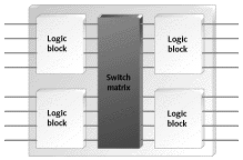
Figure 1. Internal structure of a CPLD
Figure 1 contains a block diagram of a hypothetical CPLD. Each of the four logic blocks shown there is the equivalent of one PLD. However, in an actual CPLD there may be more (or less) than four logic blocks. I've just drawn it that way for simplicity. Note also that these logic blocks are themselves comprised of macro cells and interconnect wiring, just like an ordinary PLD.
Unlike the programmable interconnect within a PLD, the switch matrix within a CPLD may or may not be fully connected. In other words, some of the theoretically possible connections between logic block outputs and inputs may not actually be supported within a given CPLD. The effect of this is most often to make 100% utilization of the macrocells very difficult to achieve. Some hardware designs simply won't fit within a given CPLD, even though there are sufficient logic gates and flip-flops available.
Field Programmable Gate Arrays (FPGAs) can be used to implement just about any hardware design. One common use is to prototype a lump of hardware that will eventually find its way into an ASIC. However, there is nothing to say that the FPGA can't remain in the final product. Whether or not it does will depend on the relative weights of development cost and production cost for a particular project. (It costs significantly more to develop an ASIC, but the cost per chip may be lower in the long run. The cost tradeoff involves expected number of chips to be produced and the expected likelihood of hardware bugs and/or changes. This makes for a rather complicated cost analysis, to say the least.)
The development of the FPGA was distinct from the PLD/CPLD evolution just described. This is apparent when you look at the structures inside. Figure 2 illustrates a typical FPGA architecture. There are three key parts of its structure: logic blocks, interconnect, and I/O blocks. The I/O blocks form a ring around the outer edge of the part. Each of these provides individually selectable input, output, or bi-directional access to one of the general-purpose I/O pins on the exterior of the FPGA package. Inside the ring of I/O blocks lies a rectangular array of logic blocks. And connecting logic blocks to logic blocks and I/O blocks to logic blocks is the programmable interconnect wiring.
| Are you interested in this topic.Then mail to us immediately to get the full report.
email :- contactv2@gmail.com |
